 |
| October 13, 2020 | Volume 16 Issue 39 |
Mechanical News & Products

Designfax weekly eMagazine

Archives
Partners
Manufacturing Center
Product Spotlight
Modern Applications News
Metalworking Ideas For
Today's Job Shops
Tooling and Production
Strategies for large
metalworking plants
Engineer's Toolbox: How to design the optimum hinge
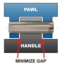 Although many pin styles are available, Coiled Spring Pins are particularly well suited for
use in both friction- and free-fit hinges. To achieve optimum long-term hinge performance,
designers should observe these helpful design guidelines from SPIROL.
Although many pin styles are available, Coiled Spring Pins are particularly well suited for
use in both friction- and free-fit hinges. To achieve optimum long-term hinge performance,
designers should observe these helpful design guidelines from SPIROL.
Read the full article.
Innovative new robo welding gun
 Comau's newest N-WG welding gun is designed for high-speed spot welding for traditional, hybrid, and electric vehicles, in addition to general industry sectors. It features a patented, single-body architecture that enables rapid reconfiguration between welding types and forces, and it delivers consistent performance across a broad range of applications, including steel and (soon) aluminum welding. It supports both X and C standard gun configurations, has fast arm exchange, and universal mounting options. It is fully compatible with major robot brands and represents a significant advancement in spot welding performance and cost efficiency.
Learn more.
What's a SLIC Pin®? Pin and cotter all in one!
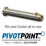 The SLIC Pin (Self-Locking Implanted Cotter Pin) from Pivot Point is a pin and cotter all in one. This one-piece locking clevis pin is cost saving, fast, and secure. It functions as a quick locking pin wherever you need a fast-lock function. It features a spring-loaded plunger that functions as an easy insertion ramp. This revolutionary fastening pin is very popular and used successfully in a wide range of applications.
Learn more.
Engineering challenge: Which 3D-printed parts will fade?
 How does prolonged exposure to intense UV light impact 3D-printed plastics? Will they fade? This is what Xometry's Director of Application Engineering, Greg Paulsen, set to find out. In this video, Paulsen performs comprehensive tests on samples manufactured using various additive processes, including FDM, SLS, SLA, PolyJet, DLS, and LSPc, to determine their UV resistance. Very informative. Some results may surprise you.
View the video.
Copper filament for 3D printing
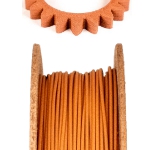 Virtual Foundry, the company that brought us 3D-printable lunar regolith simulant, says its popular Copper Filamet™ (not a typo) is "back in stock and ready for your next project." This material is compatible with any open-architecture FDM/FFF 3D printer. After sintering, final parts are 100% pure copper. Also available as pellets. The company says this is one of the easiest materials to print and sinter. New Porcelain Filamet™ available too.
Learn more and get all the specs.
Copper foam -- so many advantages
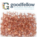 Copper foam from Goodfellow combines the outstanding thermal conductivity of copper with the structural benefits of a metal foam. These features are of particular interest to design engineers working in the fields of medical products and devices, defense systems and manned flight, power generation, and the manufacture of semiconductor devices. This product has a true skeletal structure with no voids, inclusions, or entrapments. A perennial favorite of Designfax readers.
Learn more.
Full-color 3D-printing Design Guide from Xometry
 With Xometry's PolyJet 3D-printing service, you can order full-color 3D prints easily. Their no-cost design guide will help you learn about different aspects of 3D printing colorful parts, how to create and add color to your models, and best practices to keep in mind when printing in full color. Learn how to take full advantage of the 600,000 unique colors available in this flexible additive process.
Get the Xometry guide.
Tech Tip: How to create high-quality STL files for 3D prints
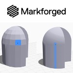 Have you ever 3D printed a part that had flat spots or faceted surfaces where smooth curves were supposed to be? You are not alone, and it's not your 3D printer's fault. According to Markforged, the culprit is likely a lack of resolution in the STL file used to create the part.
Read this detailed and informative Markforged blog.
Test your knowledge: High-temp adhesives
 Put your knowledge to the test by trying to answer these key questions on how to choose the right high-temperature-resistant adhesive. The technical experts from Master Bond cover critical information necessary for the selection process, including questions on glass transition temperature and service temperature range. Some of the answers may surprise even the savviest of engineers.
Take the quiz.
Engineer's Toolbox: How to pin a shaft and hub assembly properly
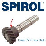 One of the primary benefits of using a coiled spring pin to affix a hub or gear to a shaft is the coiled pin's ability to prevent hole damage. Another is the coiled pin absorbs wider hole tolerances than any other press-fit pin. This translates to lower total manufacturing costs of the assembly. However, there are a few design guidelines that must be adhered to in order to achieve the maximum strength of the pinned system and prevent damage to the assembly.
Read this very informative SPIROL article.
What's new in Creo Parametric 11.0?
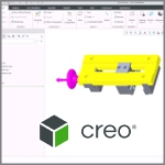 Creo Parametric 11.0 is packed with productivity-enhancing updates, and sometimes the smallest changes make the biggest impact in your daily workflows. Mark Potrzebowski, Technical Training Engineer, Rand 3D, runs through the newest functionality -- from improved surface modeling tools to smarter file management and model tree navigation. Videos provide extra instruction.
Read the full article.
What's so special about wave springs?
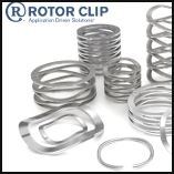 Don't settle for ordinary springs. Opt for Rotor Clip wave springs. A wave spring is a type of flat wire compression spring characterized by its unique waveform-like structure. Unlike traditional coil springs, wave springs offer an innovative solution to complex engineering challenges, producing forces from bending, not torsion. Their standout feature lies in their ability to compress and expand efficiently while occupying up to 50% less axial space than traditional compression springs. Experience the difference Rotor Clip wave springs can make in your applications today!
View the video.
New Standard Parts Handbook from JW Winco
 JW Winco's printed Standard Parts Handbook is a comprehensive 2,184-page reference that supports designers and engineers with the largest selection of standard parts categorized into three main groups: operating, clamping, and machine parts. More than 75,000 standard parts can be found in this valuable resource, including toggle clamps, shaft collars, concealed multiple-joint hinges, and hygienically designed components.
Get your Standard Parts Handbook today.
Looking to save space in your designs?
 Watch Smalley's quick explainer video to see how engineer Frank improved his product designs by switching from traditional coil springs to compact, efficient wave springs. Tasked with making his products smaller while keeping costs down, Frank found wave springs were the perfect solution.
View the video.
Top die casting design tips
 You can improve the design and cost of your die cast parts with these top tips from Xometry's Joel Schadegg. Topics include: Fillets and Radii, Wall Thicknesses, Ribs and Metal Savers, Holes and Windows, Parting Lines, and more. Follow these recommendations so you have the highest chance of success with your project.
Read the full Xometry article.
MIT tries turning diamond metallic to make next-gen semiconductor

Researchers have discovered a way to transform the electronic properties of nanoscale needles of diamond. [Image: MIT News]
Long known as the hardest of all natural materials, diamonds are also exceptional thermal conductors and electrical insulators. Now, researchers have discovered a way to tweak tiny needles of diamond in a controlled way to transform their electronic properties, dialing them from insulating, through semiconducting, all the way to highly conductive, or metallic. This can be induced dynamically and reversed at will, with no degradation of the diamond material.
The research, though still at an early proof-of-concept stage, may open up a wide array of potential applications, including new kinds of broadband solar cells, highly efficient LEDs and power electronics, and new optical devices or quantum sensors, the researchers say.
Their findings, which are based on simulations, calculations, and previous experimental results, are reported in the Proceedings of the National Academy of Sciences in October 2020. The paper is by MIT Professor Ju Li and graduate student Zhe Shi; Principal Research Scientist Ming Dao; Professor Subra Suresh, who is president of Nanyang Technological University in Singapore as well as former dean of engineering and Vannevar Bush Professor Emeritus at MIT; and Evgenii Tsymbalov and Alexander Shapeev at the Skolkovo Institute of Science and Technology in Moscow.
The team used a combination of quantum mechanical calculations, analyses of mechanical deformation, and machine learning to demonstrate that the phenomenon, long theorized as a possibility, really can occur in nanosized diamond.
The concept of straining a semiconductor material such as silicon to improve its performance found applications in the microelectronics industry more than two decades ago. However, that approach entailed small strains on the order of about 1%. Li and his collaborators have spent years developing the concept of elastic strain engineering. This is based on the ability to cause significant changes in the electrical, optical, thermal, and other properties of materials simply by deforming them -- putting them under moderate to large mechanical strain, enough to alter the geometric arrangement of atoms in the material's crystal lattice, but without disrupting that lattice.
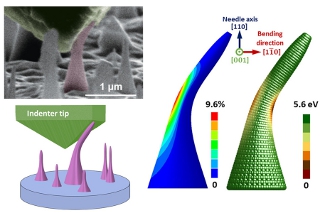
Tiny needles of diamond are strained by bending, as seen in this electron microscope image, top left. Computer simulations show the effects, with normal insulating properties in green, and areas with metallic properties, never seen before in diamond, in deep red. [Image: Courtesy of the researchers. Edited by MIT News]
In a major advance in 2018, a team led by Suresh, Dao, and Yang Lu from the City University of Hong Kong showed that tiny needles of diamond, just a few hundred nanometers across, could be bent without fracture at room temperature to large strains. They were able to repeatedly bend these nanoneedles to tensile strain as much as 10%; the needles can then return intact to their original shape.
Key to this work is a property known as bandgap, which essentially determines how readily electrons can move through a material. This property is thus key to the material's electrical conductivity. Diamond normally has a very wide bandgap of 5.6 electron volts, meaning that it is a strong electrical insulator that electrons do not move through readily. In their latest simulations, the researchers show that diamond's bandgap can be gradually, continuously, and reversibly changed, providing a wide range of electrical properties, from insulator through semiconductor to metal.
"We found that it's possible to reduce the bandgap from 5.6 electron volts all the way to zero," Li says. "The point of this is that if you can change continuously from 5.6 to 0 electron volts, then you cover all the range of bandgaps. Through strain engineering, you can make diamond have the bandgap of silicon, which is most widely used as a semiconductor, or gallium nitride, which is used for LEDs. You can even have it become an infrared detector or detect a whole range of light all the way from the infrared to the ultraviolet part of the spectrum."
"The ability to engineer and design electrical conductivity in diamond without changing its chemical composition and stability offers unprecedented flexibility to custom design its functions," says Suresh. "The methods demonstrated in this work could be applied to a broad range of other semiconductor materials of technological interest in mechanical, microelectronics, biomedical, energy, and photonics applications through strain engineering."
So, for example, a single tiny piece of diamond, bent so that it has a gradient of strain across it, could become a solar cell capable of capturing all frequencies of light on a single device -- something that currently can only be achieved through tandem devices that couple different kinds of solar cell materials together in layers to combine their different absorption bands. These might someday be used as broad-spectrum photodetectors for industrial or scientific applications.
One constraint, which required not only the right amount of strain but also the right orientation of the diamond's crystalline lattice, was to prevent the strain from causing the atomic configuration to cross a tipping point and turning into graphite, the soft material used in pencils.
The process can also make diamond into two types of semiconductors, either "direct" or "indirect" bandgap semiconductors, depending on the intended application. For solar cells, for example, direct bandgaps provide a much more efficient collection of energy from light, allowing them to be much thinner than materials such as silicon, whose indirect bandgap requires a much longer pathway to collect a photon's energy.
The process could be relevant for a wide variety of potential applications, Li suggests, such as for highly sensitive quantum-based detectors that use defects and dopant atoms in a diamond. "Using strain, we can control the emission and absorption levels of these point defects," he says, allowing novel ways of controlling their electronic and nuclear quantum states.
But given the great variety of conditions made possible by the different dimensions of strain variations, Li says, "if we have a particular application in mind, then we could optimize toward that application target. And what is nice about the elastic straining approach is that it is dynamic," so that it can be continuously varied in real time as needed.
This early-stage proof-of-concept work is not yet at the point where they can begin to design practical devices, the researchers say, but with the ongoing research they expect that practical applications could be possible, partly because of promising work being done around the world on the growth of homogeneous diamond materials.
The work was supported by the U.S. Office of Naval Research.
Source: MIT
Published October 2020
Rate this article
View our terms of use and privacy policy