 |
| May 23, 2023 | Volume 19 Issue 20 |
Mechanical News & Products

Designfax weekly eMagazine

Archives
Partners
Manufacturing Center
Product Spotlight
Modern Applications News
Metalworking Ideas For
Today's Job Shops
Tooling and Production
Strategies for large
metalworking plants
Engineer's Toolbox: How to design the optimum hinge
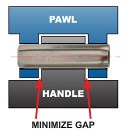 Although many pin styles are available, Coiled Spring Pins are particularly well suited for
use in both friction- and free-fit hinges. To achieve optimum long-term hinge performance,
designers should observe these helpful design guidelines from SPIROL.
Although many pin styles are available, Coiled Spring Pins are particularly well suited for
use in both friction- and free-fit hinges. To achieve optimum long-term hinge performance,
designers should observe these helpful design guidelines from SPIROL.
Read the full article.
Innovative new robo welding gun
 Comau's newest N-WG welding gun is designed for high-speed spot welding for traditional, hybrid, and electric vehicles, in addition to general industry sectors. It features a patented, single-body architecture that enables rapid reconfiguration between welding types and forces, and it delivers consistent performance across a broad range of applications, including steel and (soon) aluminum welding. It supports both X and C standard gun configurations, has fast arm exchange, and universal mounting options. It is fully compatible with major robot brands and represents a significant advancement in spot welding performance and cost efficiency.
Learn more.
What's a SLIC Pin®? Pin and cotter all in one!
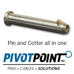 The SLIC Pin (Self-Locking Implanted Cotter Pin) from Pivot Point is a pin and cotter all in one. This one-piece locking clevis pin is cost saving, fast, and secure. It functions as a quick locking pin wherever you need a fast-lock function. It features a spring-loaded plunger that functions as an easy insertion ramp. This revolutionary fastening pin is very popular and used successfully in a wide range of applications.
Learn more.
Engineering challenge: Which 3D-printed parts will fade?
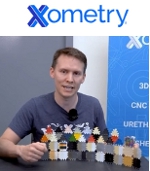 How does prolonged exposure to intense UV light impact 3D-printed plastics? Will they fade? This is what Xometry's Director of Application Engineering, Greg Paulsen, set to find out. In this video, Paulsen performs comprehensive tests on samples manufactured using various additive processes, including FDM, SLS, SLA, PolyJet, DLS, and LSPc, to determine their UV resistance. Very informative. Some results may surprise you.
View the video.
Copper filament for 3D printing
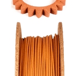 Virtual Foundry, the company that brought us 3D-printable lunar regolith simulant, says its popular Copper Filamet™ (not a typo) is "back in stock and ready for your next project." This material is compatible with any open-architecture FDM/FFF 3D printer. After sintering, final parts are 100% pure copper. Also available as pellets. The company says this is one of the easiest materials to print and sinter. New Porcelain Filamet™ available too.
Learn more and get all the specs.
Copper foam -- so many advantages
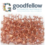 Copper foam from Goodfellow combines the outstanding thermal conductivity of copper with the structural benefits of a metal foam. These features are of particular interest to design engineers working in the fields of medical products and devices, defense systems and manned flight, power generation, and the manufacture of semiconductor devices. This product has a true skeletal structure with no voids, inclusions, or entrapments. A perennial favorite of Designfax readers.
Learn more.
Full-color 3D-printing Design Guide from Xometry
 With Xometry's PolyJet 3D-printing service, you can order full-color 3D prints easily. Their no-cost design guide will help you learn about different aspects of 3D printing colorful parts, how to create and add color to your models, and best practices to keep in mind when printing in full color. Learn how to take full advantage of the 600,000 unique colors available in this flexible additive process.
Get the Xometry guide.
Tech Tip: How to create high-quality STL files for 3D prints
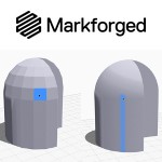 Have you ever 3D printed a part that had flat spots or faceted surfaces where smooth curves were supposed to be? You are not alone, and it's not your 3D printer's fault. According to Markforged, the culprit is likely a lack of resolution in the STL file used to create the part.
Read this detailed and informative Markforged blog.
Test your knowledge: High-temp adhesives
 Put your knowledge to the test by trying to answer these key questions on how to choose the right high-temperature-resistant adhesive. The technical experts from Master Bond cover critical information necessary for the selection process, including questions on glass transition temperature and service temperature range. Some of the answers may surprise even the savviest of engineers.
Take the quiz.
Engineer's Toolbox: How to pin a shaft and hub assembly properly
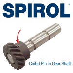 One of the primary benefits of using a coiled spring pin to affix a hub or gear to a shaft is the coiled pin's ability to prevent hole damage. Another is the coiled pin absorbs wider hole tolerances than any other press-fit pin. This translates to lower total manufacturing costs of the assembly. However, there are a few design guidelines that must be adhered to in order to achieve the maximum strength of the pinned system and prevent damage to the assembly.
Read this very informative SPIROL article.
What's new in Creo Parametric 11.0?
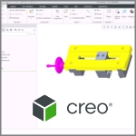 Creo Parametric 11.0 is packed with productivity-enhancing updates, and sometimes the smallest changes make the biggest impact in your daily workflows. Mark Potrzebowski, Technical Training Engineer, Rand 3D, runs through the newest functionality -- from improved surface modeling tools to smarter file management and model tree navigation. Videos provide extra instruction.
Read the full article.
What's so special about wave springs?
 Don't settle for ordinary springs. Opt for Rotor Clip wave springs. A wave spring is a type of flat wire compression spring characterized by its unique waveform-like structure. Unlike traditional coil springs, wave springs offer an innovative solution to complex engineering challenges, producing forces from bending, not torsion. Their standout feature lies in their ability to compress and expand efficiently while occupying up to 50% less axial space than traditional compression springs. Experience the difference Rotor Clip wave springs can make in your applications today!
View the video.
New Standard Parts Handbook from JW Winco
 JW Winco's printed Standard Parts Handbook is a comprehensive 2,184-page reference that supports designers and engineers with the largest selection of standard parts categorized into three main groups: operating, clamping, and machine parts. More than 75,000 standard parts can be found in this valuable resource, including toggle clamps, shaft collars, concealed multiple-joint hinges, and hygienically designed components.
Get your Standard Parts Handbook today.
Looking to save space in your designs?
 Watch Smalley's quick explainer video to see how engineer Frank improved his product designs by switching from traditional coil springs to compact, efficient wave springs. Tasked with making his products smaller while keeping costs down, Frank found wave springs were the perfect solution.
View the video.
Top die casting design tips
 You can improve the design and cost of your die cast parts with these top tips from Xometry's Joel Schadegg. Topics include: Fillets and Radii, Wall Thicknesses, Ribs and Metal Savers, Holes and Windows, Parting Lines, and more. Follow these recommendations so you have the highest chance of success with your project.
Read the full Xometry article.
OLEDs found in smartphone screens can be used to map magnetic fields
Hand-held magnetic field imaging equipment could be used in construction safety and medical diagnostics.
Smartphones could one day become portable quantum sensors thanks to a new chip-scale approach that uses organic light-emitting diodes (OLEDs) to image magnetic fields, with significant implications for use in healthcare and industry settings.
Researchers from the University of New South Wales' (UNSW Sydney, Australia) ARC Center of Excellence in Exciton Science have demonstrated that OLEDs, a type of semiconductor material commonly found in flat-screen televisions, smartphone screens, and other digital displays, can be harnessed to map magnetic fields.
The latest research, led by Dr. Rugang Geng and Professor Dane McCamey from the UNSW School of Physics, has been detailed in Nature Communications.
"Our findings show that OLEDs, a commercially available technology, can be used not only for displays and lighting, but also for quantum sensing and magnetic field imaging by integrating a small piece of microwave electronics," says Geng, the first author of the study. "If this technology is properly developed, people could simply use their smartphones to map the magnetic fields around them, for example to spot defects in diamonds or jewelry. This also has applications in industry, such as finding defects in construction materials or as a biomedical sensor."
How does the technology work?
OLEDs are a newer display technology that provides some of the best-quality screens in smartphones and TVs.
"The basic working principle of an OLED device is that when a voltage is applied, electrons and holes are injected into different layers of the device," says Geng. "When the electrons and holes meet in the central layer, they form "excitons," which emit visible light when they decay, and that's what makes OLEDs useful as displays and lighting sources."
This light emission process exploits the charge characteristics of electrons, which have a negative charge, and holes, which have a positive charge. They both also have another intrinsic property called spin.
This spin either points up or down and is very sensitive to external magnetic fields. In fact, it can flip-flop (or switch direction) under magnetic resonance conditions.
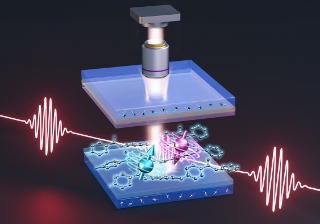
The spin property of electrons and holes, which meet in the middle layer of the device, either point up or down and are very sensitive to external magnetic fields. [Credit: UNSW Sydney researchers.]
"By measuring the signal change, both in electric current and emission light, induced by such a flip-flop, we are able to detect the strength of any magnetic field the device is exposed to," says Geng.
By integrating an OLED with a microwave resonator, Geng, McCamey, and their colleagues have generated a tiny oscillating magnetic field across the OLED device, allowing each individual pixel of the OLED screen to act as a small magnetic field sensor.
"We weren't surprised at the result -- we have been pursuing this for a few years," says McCamey. "But we were surprised at the resolution of the images we could make -- we can see details on sub-micron-length scales, similar to the size of a bacteria or neuron."
Commercialization and everyday uses
This latest research represents the next step in the development of magnetic field imaging equipment. Existing quantum sensing and magnetic field imaging equipment tends to be large and expensive, requiring either additional power from a high-powered laser, or extremely low temperatures. Under these conditions, the device integration potential and commercial scalability is limited.
However, the new technique developed by the team can function at a microchip scale and doesn't require input from a laser, showing great potential for applications in scientific research, industry, and medicine.
"Next, we hope to improve the overall performance of the device including optimizing the device architecture and exploring other techniques that can significantly increase the field sensitivity," says Geng. "We are also exploring collaborations with OLED technology companies, as their experience at moving devices from the lab to commercial products will help accelerate translation of this technology."
Source: The University of New South Wales (UNSW Sydney)
Published May 2023
Rate this article
View our terms of use and privacy policy